Microvia Electroplating Additives for Next-generation High-density-interconnect Substrate
Microvia in high-density-interconnect (HDI) substrate for system integration offers a number of advantages, such as performance improvement and product miniaturisation. Electroplating additives are essential for copper electrodeposition fabrication of microvias in HDI substrate. The technology-intensive additives can only be provided by a few electronic material companies and at a very high profit margin. As the trend of miniaturisation and increased functionality of advanced electronics continues, higher technical requirements including thinner surface deposition and smaller dimple are introduced for the next-generation microvia (<75µm) fabrication, and hence new electroplating additives are in high market demand.
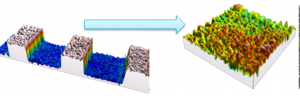
Guided by our mechanism-based electroplating simulation software, ASTRI has developed a methodology for fast screening of electroplating additive candidates to shorten the material development cycle time and reduce the development cost. Based on this methodology, a series of new electroplating suppressors with tuned molecular weight distribution and new electroplating levelers with lower mass-to-charge ratio and balanced functional groups have been developed to meet the above-mentioned requirements for microvia fabrication and to achieve better electroplating performances than that of existing commercial additives.
Features
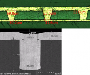
- Dimple size less than 5µm; Cu thickness as thin as 10µm
- High T/P performance of through hole filling
- Excellent adhesion, uniformity and reliability
Applications
- High density, multi-layer, ultra-thin HDI PCB for advanced electronic devices (for examples, smartphones, wearable devices, etc.)
- Fine pitch IC substrate for high I/O and high speed chips (including micro-processors, memory chips, etc.)
Etching additives for Next-generation High-density-interconnect Substrate
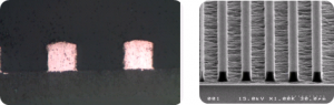
The demand for finer line/space pattern formation of high density interconnect (HDI) substrates has replaced conventional subtractive circuit formation with semi-additive process (SAP) and modified semi-additive process (MSAP) technologies as the mainstream circuit production technologies. These advanced technologies however still face many challenges and have room for improvement. Two of the challenges for MSAP technologies are copper electrodeposition for signal line formation, blind microvia and through hole filling, and the flash etching which is to finalize the circuit formation by removing the copper seed layer through differential etching.
ASTRI has developed its novel etching additives to overcome the severe undercut issue due to narrower and higher aspect-ratio etch channels for fine circuitry. The newly designed banking agent can enhance efficiency of etching inhibition at channel sidewall. An accelerator is employed at the channel bottom to speed up the etching rate and working hand in hand with the banking agent to minimize undercut. In addition, a new electrodeposition recipe has been developed for both blind microvia and through hole filling to meet the market demand on one electrodeposition solution/cell for multi-tasks. The development of the etching additives and the recipes can be widely used in high-density interconnect applications.
Features
• H2O2, H2SO4 based flash etchant for fine circuit etching
• Suitable for SAP/MSAP process
• L/S can reach 15µm/15µm
• High etch factor, no undercut
• Short etch time, high etch rate
• Good surface morphology and trace uniformity
Applications
• High density, multi-layer, ultra-thin HDI PCB for advanced electronic devices (smartphones, wearable devices, etc.)
• Fine pitch IC substrate for high I/O and high speed chips (micro processors, memory chips, etc.)